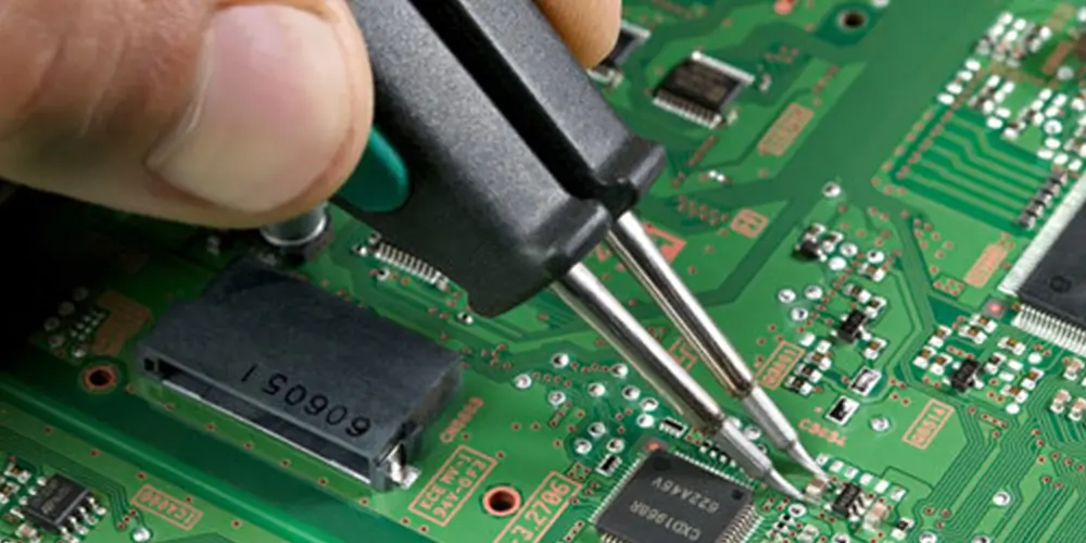
“Having a cross-functional team and an electronics lab on site enables faster usability testing and overall faster time to market.”
Aaron Russell
Extracting inefficiencies from product development workflows has always been important, but even more so now as production times get squeezed in an effort to stay ahead of the competition. To speed up the entire prototyping process, more companies are establishing specialised electronic labs on site that work closely with core product design and development teams.
For ide Group, having an integrated, cross-functional team and electronics lab on site means speedy turnaround times for prototype manufacturing, allowing faster integration of printed circuit boards (PCB’s) with custom enclosures to produce small batch production runs. This enables faster usability testing and overall faster time to market.
Here are three other ways electronic engineers are speeding up turnarounds for prototype builds.
1. Applying targeted design spin processes
When designing complex electronic systems for product integration, a lot of people still take the old approach of building their product’s entire electronics system, then seeing if it works. Part of the reason this approach is still around is that there is a customer perception (based on some reality) that multiple design spins or PCB layout changes are an expensive way to do development. There is an Non recoverable Engineering (NRE) cost to cutting new stencils for the manufacture of each new layout.
More spins don’t necessarily mean better products, but as products become more complex and connected, those who can catch mistakes early and often through experimentation will be the ones who have the ability to produce much better products with greater long term potential. To do that you need to be able to handle the development of quick electronic prototypes.
2. Building tighter bonds between design and engineering
Managing more than one environment requires more time and money. Product development teams that have integrated electronic engineering expertise can flow ideas much more quickly and freely, tightening the margin for error and lessening the risk of a project puttering to a halt.
When electronic engineers are integrated across the design and development process and using modern CAD collaboration tools, it cuts down the overhead of interdisciplinary communication and allows nimble exploration of design concepts. Design teams can segment the problem into design functions rather than disciplinary functions, allowing each part to be tested for function and usability much earlier.
3. Creating unique tribal knowledge
Product developers, designers and electronic engineers all have a different way of communicating. What one engineer thinks is great might not translate well into the design of the product and vice versa, making it very difficult to commercialise.
Yet, when all teams are in close proximity, working towards the same goal and speaking the same design language, incredible things can happen. Cross functional, integrated teams begin to develop their own unique tribal knowledge that can give them a competitive edge. Designs work as a whole package and products are produced with the same goal and end in sight.
At ide, we’re always asking each other questions and cross pollinating expertise in new and unique ways. Because we’re all working together with access to the right tools, simple questions can be tested and prototyped quickly, allowing us to fail fast and ultimately produce more meaningful products that can make a difference.


